
Synthetic Diamond Market Dynamics
authored by @jamesdumar.com | Identity: did:plc:7vknci6jk2jqfwsq6gkzu
The integration of synthetic diamond into chip and electronics manufacturing represents one of the most consequential shifts in advanced materials engineering. Long pursued as the “ultimate semiconductor” due to its peerless physical and thermal properties, synthetic diamond is transitioning from an exotic laboratory curiosity to a critical high-volume substrate and thermal management asset. The new strategic framework for AI manufacturing will use synthetic diamond extensively in the program called Pax Silica.
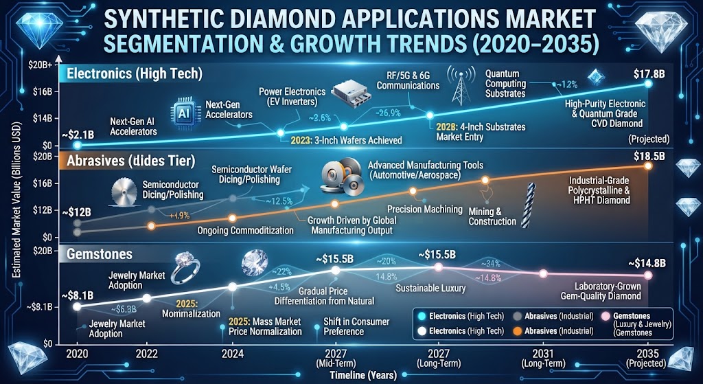
1. Size of Demand in Electronics and Semiconductor Sectors
The market footprint of synthetic diamond in electronics is divided into two primary categories: supporting materials (such as heat sinks, wafer-dicing tools, and polishing plates) and active semiconductor substrates (wafers and films used to build power electronics and high-frequency RF devices).
Overall Market Valuation: The global diamond materials for semiconductor market was valued at approximately $2.1 billion, while the broader synthetic diamond market sits near $18.1 billion (Dataintelo, 2026; IMARC Group, 2026). Driven by surging requirements for ultra-wide bandgap (UWBG) materials, the semiconductor-specific diamond market is projected to scale aggressively at a compound annual growth rate (CAGR) exceeding 26%, heading toward roughly $17.8 billion over the next decade (Dataintelo, 2026).
Power Electronics and EVs as Primary Catalysts: The electrification of transportation and industrial infrastructure serves as the primary demand engine. With electric vehicle (EV) production surpassing tens of millions of units annually, automakers require power semiconductors (inverters, onboard chargers, and DC-DC converters) capable of managing extreme voltages (400V to 800V+) with minimal thermal loss. While silicon carbide (SiC) has captured initial ground, diamond possesses a theoretical Baliga’s Figure of Merit (BFOM) over 50,000 times that of silicon, making it the theoretical pinnacle for high-power switching.
RF and 5G/6G Communications: High-frequency radio frequency (RF) devices used in defense, aerospace, and telecommunications generate immense heat densities. Synthetic diamond heat spreaders and substrates are increasingly specified to prevent thermal throttling in gallium nitride (GaN) high-electron-mobility transistors (HEMTs).
2. Impact on Manufacturing Volume
The rapid scaling of synthetic diamond demand is directly reshaping fabrication pipelines, moving the material from small-scale batch production to continuous industrial crystal growth.
CVD Scaling and Reactor Capacity: Chemical Vapor Deposition (CVD)—specifically microwave plasma CVD—has become the dominant technique for growing electronic-grade single-crystal and polycrystalline diamond films. To meet projected electronic volumes, leading materials suppliers (such as Element Six, Sumitomo Electric, and specialized startups) are scaling up multi-kW reactor capacity to produce larger-diameter wafers.
Overcoming the “Substrate Bottleneck”: Historically, the lack of native, large-area single-crystal diamond substrates throttled manufacturing volume; chips had to be patterned on tiny, expensive diamond fragments. Breakthroughs allowing the heteroepitaxial growth of diamond on foreign substrates (such as iridium/silicon) and mosaic wafer bonding are finally enabling 1-inch to 2-inch single-crystal wafers, with active R&D pushing toward 4-inch equivalents.
Integration into Standard CMOS/Fab Lines: Rather than replacing traditional silicon or compound semiconductor fabs entirely, synthetic diamond is largely being adopted in heterogeneous integration. Diamond heat spreaders are bonded directly to the topside of high-performance logic, AI accelerators, or power chips, drastically lowering junction temperatures and allowing foundries to push clock speeds and power densities higher without redesigning underlying silicon processes.
3. Impact on Pricing and Cost Trajectories
Pricing dynamics in synthetic diamond are dictated by a classic technology curve: massive yield improvements and scaling are rapidly lowering costs, though electronic-grade purity remains an expensive tier.
Historical Price Compression: A decade ago, high-purity electronic-grade diamond substrates routinely exceeded $5,000 per square centimeter. Thanks to maturation in microwave plasma CVD kinetics and improved nucleation controls, prices for commercial-grade semiconductor substrates have dropped below $1,000 per cm² for specific industrial and thermal grades (Dataintelo, 2026).
The Purity Premium: A stark bifurcation exists in the pricing model. Industrial-grade polycrystalline diamond (used for heat sinks and cutting tools) is heavily commoditized and priced relatively low by volume. Conversely, electronic-grade single-crystal diamond—which requires nitrogen and defect concentrations measured in parts per billion (ppb) to maintain carrier mobility—commands a steep premium.
Cost Parity with SiC and GaN: For diamond to displace silicon carbide in high-volume automotive lines, its $/cm² metric must eventually approach parity with mature WBG materials. Analysts note that while diamond substrate costs remain higher than SiC wafers, the system-level savings—eliminating bulky copper cooling blocks, liquid cooling loops, and thermal interface materials—often offset the initial wafer cost premium in high-end defense, aerospace, and premium EV powertrains.
The competitive landscape of synthetic diamond production for electronics is shifting rapidly from fragmented, high-cost boutique synthesis toward consolidated, industrial-grade manufacturing. Historically constrained by the microscopic size of diamond crystals (typically grown as isolated platelets measuring only a few millimeters across), key industry players have unlocked major scaling milestones.
Key Competitors and Strategic Positioning
The synthetic single-crystal diamond market is moderately consolidated, with a clear tier of market leaders dominating high-purity electronic and quantum-grade substrates, alongside a high-volume industrial cluster centered in Asia.
1. Element Six (Part of De Beers Group)
Role: Global leader in high-purity Chemical Vapor Deposition (CVD) single-crystal and polycrystalline diamond. Headquartered in the UK with major production facilities in the US (Gresham, Oregon), Europe, and South Africa.
Strengths: Unrivaled intellectual property in microwave plasma CVD kinetics and electronic-grade purity (maintaining nitrogen and defect concentrations in the parts-per-billion range). Element Six anchors high-end defense, quantum, and thermal-management deployments globally.
2. Orbray Co., Ltd. (Japan)
Role: Precision jewel-processing pioneer turned diamond substrate innovator.
Strengths: World-renowned expertise in mechanical cutting, grinding, and polishing. Orbray has pioneered advanced heteroepitaxial growth techniques (such as growing single-crystal diamond on cost-efficient sapphire substrates) and independent (111) diamond substrates.
3. IIa Technologies (Singapore) & Sumitomo Electric Industries (Japan)
Role: Long-standing heavyweights in high-pressure high-temperature (HPHT) and advanced CVD diamond synthesis.
Strengths: Sumitomo commands deep integration into power semiconductor supply chains, while IIa Technologies operates massive commercial-scale growth reactors primarily utilized for both high-grade optical windows and electronics.
4. High-Volume Industrial and Regional Specialists (China, US, and Europe)
China (e.g., Henan Huanghe Whirlwind, Henan Liliang Diamond): Dominates the global output of bulk synthetic diamond by volume (primarily HPHT and structural/thermal grades), increasingly expanding into large-scale industrial heat sinks for AI hardware.
Europe & US Startups (e.g., Diamond Foundry, Diamfab): Diamond Foundry operates major low-emissions CVD facilities (such as its plant in Trujillo, Spain), while French startup Diamfab focuses on diamond epitaxy for power devices.
Progress Toward Large-Area Single-Crystal Wafers
The defining bottleneck for diamond semiconductors has been the “sub-inch limit”—the inability to scale single-crystal lattice growth without introducing fatal structural dislocations or bowing. Recent industry milestones have shattered this barrier:
The Element Six & Orbray Alliance (3-Inch Breakthrough): Element Six and Orbray established a reproducible manufacturing process for 3-inch wafer-scale single-crystal (WSC) diamond. This represents a massive step change in size uniformity compared to historical sub-inch chips. Concurrently, the partners are laying the groundwork for 4-inch substrates while prepping 2-inch thermal-bonding wafers for volume production at Element Six’s Oregon facility.
Independent (111) Substrates: Orbray achieved standalone production milestones for large-diameter (111)-oriented single-crystal diamond substrates (such as 20mm × 20mm formats), explicitly designed for quantum and high-power switching applications.
Mosaic Wafer and Heteroepitaxial Scaling: To bypass the physical limits of native diamond seed growth, developers are utilizing mosaic stitching (joining smaller single-crystal tiles seamlessly) and heteroepitaxy on foreign bases like iridium/silicon or sapphire. This paves the way for standardizing 2-inch and 4-inch handling protocols that align with legacy semiconductor fabrication tools.
The rapid escalation of artificial intelligence workload intensities has turned thermal management into the primary engineering bottleneck for high-end silicon. As leading-edge AI accelerators and GPU architectures (such as Nvidia’s Blackwell, Rubin, and equivalent AMD platforms) push power envelopes past 1,000 to 2,000 watts per package, localized chip heat fluxes have exceeded the limits of traditional copper-and-water setups.
Synthetic diamond—boasting a room-temperature thermal conductivity roughly 5 times that of copper and 11 times that of aluminum—is being integrated directly into AI packaging lines to eliminate micro-hotspots and prevent performance-crippling thermal throttling.
1. Architectural Integration Strategies in AI Hardware
Semiconductor designers and hardware vendors are deploying synthetic diamond across distinct layers of the packaging hierarchy:
Diamond-Copper Composite Baseplates: Rather than replacing entire heat sinks with cost-prohibitive pure single-crystal diamond, major hardware manufacturers (such as MSI in collaboration with Nvidia ecosystems) utilize diamond-copper (or diamond-silicon carbide) composites. These composite baseplates fuse diamond particles into a metal matrix, achieving a high thermal conductivity that outstrips pure copper while maintaining a thermal expansion coefficient closely matched to silicon. This prevents the chip from cracking under sudden, extreme thermal cycling.
Direct-to-Die “Skin-to-Skin” Spreaders: Traditional heat spreaders require thermally conductive pastes or greases, which introduce microscopic air gaps and thermal resistance. Because synthetic diamond is an exceptional electrical insulator, it can be placed into direct physical contact with the bare silicon die or High-Bandwidth Memory (HBM) stacks. This allows heat to be absorbed instantly at the source without risking electrical shorts.
Low-Temperature On-Chip Growth: Cutting-edge research and manufacturing trials are bypassing traditional bonding by growing polycrystalline or nanocrystalline diamond films directly onto functional semiconductor structures (such as GaN power blocks or silicon interposers) via low-temperature Chemical Vapor Deposition (CVD). This drops junction temperatures by tens of degrees Celsius right at the transistor level.
2. Impact on Data Center Cooling Paradigms
The integration of synthetic diamond into GPUs does more than just protect individual chips; it fundamentally alters data center infrastructure requirements:
Mitigating the 1,000W+ Wall: As single-chip power consumption targets scale upward, conventional direct-to-chip liquid cold plates approach their practical conduction limits. Diamond spreaders pull heat away from active transistors so rapidly that they dramatically lower internal thermal resistance.
Unlocking Thin-Film Phase-Change Cooling: A breakthrough attribute of diamond-backed architecture is its ability to raise the temperature at the ultimate cooling boundary. By redistributing heat so efficiently, the exterior cooling surface becomes hot enough to trigger micro-scale boiling (thin-film evaporation) at near-atmospheric pressure. This shifts systems from heavy water-circulation loops to high-efficiency two-phase spray cooling, drastically reducing the volume of water required per data center rack.
Integrating synthetic diamond thermal management into enterprise AI servers shifts traditional server economics. While adding an engineered diamond component introduces an initial cost premium, system-level architecture analysis shows that it yields dramatic efficiencies in the overall bill of materials (BOM) and substantially protects manufacturing and operational yields.
1. Impact on the Bill of Materials (BOM)
At first glance, synthetic diamond is a high-cost component compared to standard copper blocks or aluminum extrusion heatsinks. However, when evaluated at the total server rack level, the financial equation changes:
Modest Server-Level Cost Adder: Industry evaluations indicate that incorporating bondable CVD diamond spreaders or advanced composite heat sinks typically introduces a marginal component-level cost adder (often estimated at under 5% of the total high-end accelerator board cost).
Offsets in Balance-of-Plant Hardware: The exceptional thermal conductivity of diamond (1,000 to 2,800 W/mK) eliminates the need for complex, heavy auxiliary cooling infrastructure. By dropping peak junction temperatures by 50°C to 52°C locally, diamond heat spreaders allow manufacturers to substitute bulky multi-phase liquid-cooling loops, exotic thermal interface pastes, and multi-layered copper vapor chambers with streamlined, simplified designs.
Capital Efficiency (CapEx ROI): Because a diamond-cooled server can sustain dramatically higher power densities (scaling up multi-fold in performance per square foot), the total capital required to deploy equivalent AI compute clusters drops. Fewer total servers are required to achieve target FLOP thresholds, compressing rack counts and lowering facility space outlays.
2. Impact on Manufacturing and Operational Yields
In semiconductor and server packaging, “yield” refers both to the fabrication success rate of assembling dense 3D chip architectures and the long-term field reliability (preventing premature thermal burnout). Diamond integration impacts yields across three distinct phases:
Mitigating Thermal Stress and Warpage: Silicon and standard substrate materials experience destructive mechanical stress under extreme thermal expansion mismatches at 1,000W+ operational thresholds. Synthetic diamond shares a favorable thermal expansion profile close to silicon while possessing extreme structural stiffness (modulus of ~1050 GPa). This prevents micro-cracking and die delamination during high-speed thermal cycling, directly boosting assembly and packaging yields.
Eliminating Microchannel Contamination Risks: Many ultra-dense liquid cooling architectures rely on micro-machined fluid channels directly on or near the chip package, which are notoriously vulnerable to clogging from microscopic particulates in data center plumbing, resulting in catastrophic thermal runaway. Diamond’s superior conduction efficiency shifts the thermal bottleneck, allowing hardware designers to use robust, conventional fluid channels rather than microscopic, failure-prone features.
Exponential Improvements in Mean Time Between Failures (MTBF): Transistor degradation and leakage currents scale exponentially with temperature. By aggressively suppressing hotspots, synthetic diamond effectively doubles hardware lifespan for every significant drop in operating baseline temperature. For enterprise operators, this protects multi-million dollar AI infrastructure investments from premature degradation before depreciation periods conclude
The Pax Silica initiative
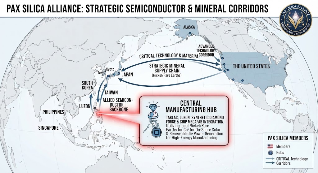
The U.S.-led economic security and technology framework focused on securing the silicon-and-mineral-to-AI supply chain—creates a profound geopolitical realignment that directly impacts the synthetic diamond market.
Because synthetic diamond is rapidly evolving from an aesthetic gem into a critical high-value industrial substrate for ultra-wide bandgap (UWBG) power electronics, RF communications, and extreme thermal management in AI hardware, it sits directly inside the strategic perimeter of Pax Silica.
The Direct Effect on the Synthetic Diamond Market
Decoupling of Substrate Supply Chains: Pax Silica explicitly targets “coercive dependencies” and non-market pricing distortion. For industrial-grade synthetic diamond (produced via HPHT and CVD), this means a hard split between aligned allied manufacturing and non-aligned high-volume producers. Sourcing diamond heat spreaders and semiconductor wafers will shift from an open global commodity market to trusted-corridor procurement.
Acceleration of Defense and AI-Driven R&D Funding: By prioritizing advanced packaging, power electronics, and high-frequency RF infrastructure, Pax Silica channels public-private co-investments into ultra-pure single-crystal diamond wafer production. This will accelerate commercial readiness, pushing single-crystal diamond past historical manufacturing bottlenecks (like size constraints and defect rates).
Bifurcation of Pricing: Gem-grade lab-grown diamonds (driven by consumer jewelry demand and loose-market overcapacity) will continue facing deflationary pricing pressures. Conversely, semiconductor-grade and thermal-grade synthetic diamond will be treated by Pax Silica as a strategic national security asset, commanding premium, secured pricing within the allied coalition.
Winners and Losers under the Pax Silica Framework
The Winners
The United States & Japan:
Why: The U.S. drives the framework architecture and holds foundational IP in advanced semiconductor architecture, while Japan (anchored by major players like Orbray and Sumitomo Electric) possesses decades of precision crystal-growing and industrial materials engineering capabilities. They become the primary architects of high-end diamond substrate integration.
Singapore & South Korea:
Why: As core signatories hosting advanced semiconductor packaging, manufacturing, and AI infrastructure hubs, they will benefit from secure, priority access to next-generation thermal management components (diamond heat spreaders and GaN-on-diamond substrates) essential for high-density AI data processing.
The Philippines (and Emerging Allied Industrial Hubs):
Why: With major designated economic corridors acting as allied manufacturing nodes under the expanded framework, secondary processing and component assembly tied to the allied semiconductor stack stand to capture massive foreign direct investment. Philippines has huge nickel production and asociated rare earths and Tarlac Luzon on the site of former military facilities is designated as the heart of this project. The net effect of processing these raw materials on shore will be a substantially reduced cost of solar electric capacity from those same materials, a reduction in cooling water consumption, and ample power for diamond forges and chip megafabs from renewable power.
Western Industrial Specialists (e.g., Element Six / De Beers Group):
Why: Element Six (operating out of the UK, South Africa, and the US) is uniquely positioned. As a dominant force in both industrial synthetic diamond and electronic-grade single crystals, they align seamlessly with allied supply-chain security mandates.
The Losers
Non-Aligned High-Volume Producers (Primarily China):
Why: China currently commands a massive share of global HPHT industrial diamond mass-production capacity (largely for abrasives and lower-tier applications). Under Pax Silica’s security perimeter, Chinese producers face total exclusion from trusted allied semiconductor and AI hardware supply chains, cutting them off from the highest-value end-markets for single-crystal electronic substrates.
Unaligned Regional Manufacturing Hubs:
Why: Countries or regional suppliers that fail to secure formal alignment or integration into the Pax Silica framework risk being relegated to unverified, low-margin tiers. They will be frozen out of joint-venture capital, advanced equipment access (such as specialized microwave plasma CVD reactors), and proprietary material-science transfers.
Traditional Gem-Only Lab-Grown Producers:
Why: Producers who rely entirely on jewelry-grade output without the technical capability to pivot toward electronic- or thermal-grade diamond specifications will suffer as capital, subsidies, and strategic attention migrate entirely toward the high-margin semiconductor sector.